|
Charge sensitive amplifiers used in radiation measurement are required to provide low noise, high gain, and fast rise-time characteristics.
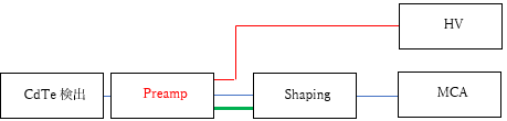
In particular, for semiconductor detectors, the characteristics obtained by the first-stage preamplifier are converted into a radiation spectrum through an amplifier and an MCA.
Since noise gain generated in the preamplifier cannot be recovered in subsequent stages, it is an extremely critical component.
When radiation such as X-rays or gamma rays enters a semiconductor detector, electron–hole pairs are generated through ionization, producing charge.
The amount of charge generated is proportional to the energy of the radiation, but it is extremely small. By using a charge-sensitive amplifier with a semiconductor detector, this charge can be extracted as a voltage pulse proportional to the radiation energy.
|
|
|
|
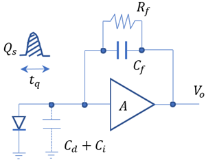
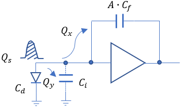
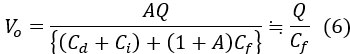
Qs is a charge pulse that is fully integrated by the feedback capacitor Cf and converted into an output voltage Vo.
The feedback resistor Rf is connected in parallel with the feedback capacitor Cf to discharge the charge accumulated in Cf.
This prevents successive charge pulses from overlapping and causing saturation of the pulse waveform. The decay time constant is given by τ = RfCf.
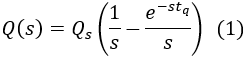
Assuming that the detector generates a constant charge over the time interval from t = 0 to tq, the input charge can be expressed by the Laplace transform as follows:
|
|
|
Here, Qs is the total charge injected between t = 0 and t = tq.
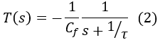
Similarly, the Laplace transform of the transfer function of the charge-sensitive amplifier is given by the following equation:
|
|
|
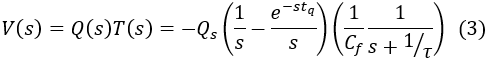
出力電圧の式は次の通りです。
|
|
|
|
さらに、tq << τと仮定すると、次のように簡略化できます。
|
|
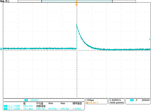
(Fig.2 チャージセンシティブアンプの出力)
|
|
チャージセンシティブアンプで重要な要素として初段に使用するデバイスですが、JFETになります。低雑音バイポーラトランジスタの場合、JFETより雑音電圧密度は低いのですが、その為にベース電流を流す必要があり、入力インピーダンスが高いチャージアンプの構成においては、並列雑音が増えてFETより全ノイズが悪化してしまいますので、選択から外れます。
OPアンプの場合、JFET入力型がありますが、雑音性能はJFET単独に劣ります。回路は非常にシンプルになるのでそれほどノイズを気にしない測定に向きます。
MOSFETは1/fノイズが大きくノイズコーナーも10kHz~1MHzと高いところにあるため使用出来ません。
JFETはゲート電流が不要なことから帰還抵抗Rfを大きくすることが可能です。またノイズコーナーも100Hz~1kHzと低く使用範囲の10kHz~10MHzは十分に低いです。低雑音化においては、初段のJFETが特に重要で高gm(相互コンダクタンス)、低Ciss(入力容量)の物を選定します。初段はエミッタ接続のフォールデットカスコード回路で受けます。
フォールデットカスコードによりダイナミックレンジの増大、高インピーダンス化を図ります。
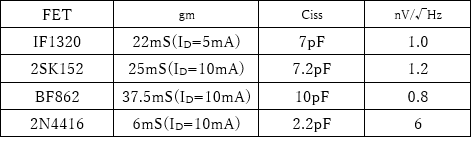
1) 初段のFETのgm(相互コンダクタンス)と入力容量Ciss
|
|
|
|
gm(相互コンダクタンス)はIDドレイン電流によって調整できます。ドレイン電流は大きいほどgmが増大しますが、消費電流の増加にも繋がるので、多チャンネルやバッテリー装置の場合は制約を受けます。FETの等価雑音抵抗はRFET≒1/gmとなるので一般的にgmが大きいほど低雑音になります。その為JFETを厳選してまでもという製品も存在します。
CissはFETの入力容量でチャージセンシティブアンプの入力容量Ciに大きな影響を与えます。発生した電荷QSは、QxとQyに分配されて流れます。S/Nを向上させるには電荷をなるべくA・Cfに流すためにA(オープンループゲイン)を十分に大きくします。Cfは電圧変換のゲインでもあるので、大きくはできません。残されたCiを極力小さくする事で、Qxへの分配を最大化させます。
|
|
|
|
Qyに流れる電荷は、検出器の容量Cdとチャージセンシティブアンプの入力容量Ciに流れ込み、S/Nを悪化させます。検出器の容量が小さい場合は、Ciができるだけ小さい事が重要となり、検出器の容量が大きい場合は、gmを大きくして低雑音にする必要があります。また、Cissが小さいFETは高速な立ち上がり特性を持ちます。
2) 帰還コンデンサCfと帰還抵抗Rf
|
|
|
|
エネルギーをE,生成された電荷をQ,検出器の静電容量(Cd)とチャージセンシティブアンプの入力容量をCi、帰還抵抗をRfとした場合、オープンループゲインAが十分に大きい場合、帰還コンデンサCfで決まる一定の値になります。
|
|
|
|
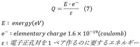
実際の放射線エネルギーに対する出力電荷Qは、下記の式であたえられます。
|
|
|
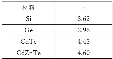
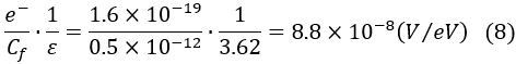
1MeVあたりの出力電圧は、Si半導体検出器で、帰還コンデンサCfが0.5pF場合
|
|
|
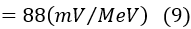
帰還コンデンサCfは1pFの場合44mV、2pFの場合22mVと出力が小さくなるので、S/Nを向上させるためにはできるだけ小さいCfを選定します。
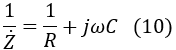
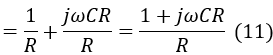
帰還抵抗Rfは大きければ大きいほどノイズは少なくなります。ここでは、CR並列抵抗のノイズについて検討します。
CR並列抵抗のアドミッタンスは、
|
|
|
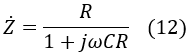
式(11)をひっくり返してインピーダンスにすると、
|
|
|
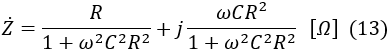
式(12)を虚数jで整理すると、
|
|
|
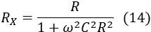
式(13)の実数部分が抵抗成分です。従って、CR並列回路の等価抵抗RXは、
|
|
|
|
抵抗の熱雑音電圧Vnは、
|
|
|
|
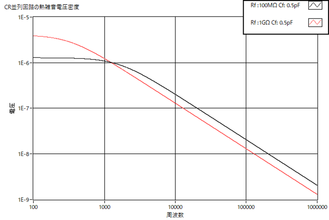
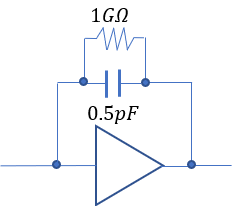
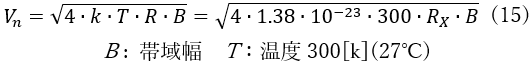
計算式(14)(15)より、帰還抵抗Rfが100MΩ、帰還コンデンサCfが0.5pFの場合と、帰還抵抗Rfが1GΩ、帰還コンデンサCfが0.5pFの場合で比べてみます。
|
|
|
|
1kHzぐらいまでの低周波数領域では、100MΩの方がノイズは少ないのですが、高周波数領域においては、1GΩの方が少なくなります。チャージセンシティブアンプで重要となる10kHz~1MHz領域のノイズの積算は、100MΩが20.3μVrmsで1GΩは12.8μVrmsです。約1.58倍になりますので1GΩにする甲斐があります。
3) オープンループゲインA
中段の増幅段、終段の出力段はトランジスタなどのディスクリートで組むより広帯域のOPアンプを使うことで小型化することが可能です。エミッター接地フォールデットカスコード+OPアンプの複合アンプの回路構成で数1000~数万のオープンループゲインを狙います。
OPアンプの選定でも重視する性能はオープンループゲインが高いことが上げられます。FET1石では、10~50倍程度しかオープンループゲインは稼げないので、特に1MHzで300倍以上は欲しい所です。雑音特性については初段のFETで決まってしまうので特に重視する必要はないのですが、心情的にローノイズOPアンプを選んでしまいますね。広帯域OPアンプであれば自ずと高速立ち上がり特性になります。
このgm、Ci、Cf、Rf、Aのパラメータを最良化した回路で設計された製品がAPG1603です。
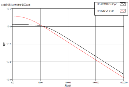
では、APG1603と他社製品(雑音特性1keV素晴らしい性能です)で雑音特性の違いがどれ程の影響があるか実際の計測で比較してみます。
まず、下記がスペックです。
|
|
|
|
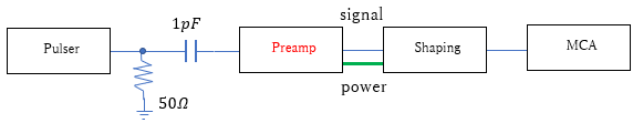
まず、パルサーを使ってカタログデータが正しいかテストしてみます。パルサーからは1MeV相当のパルス波高を発生させます。
|
|
|
|
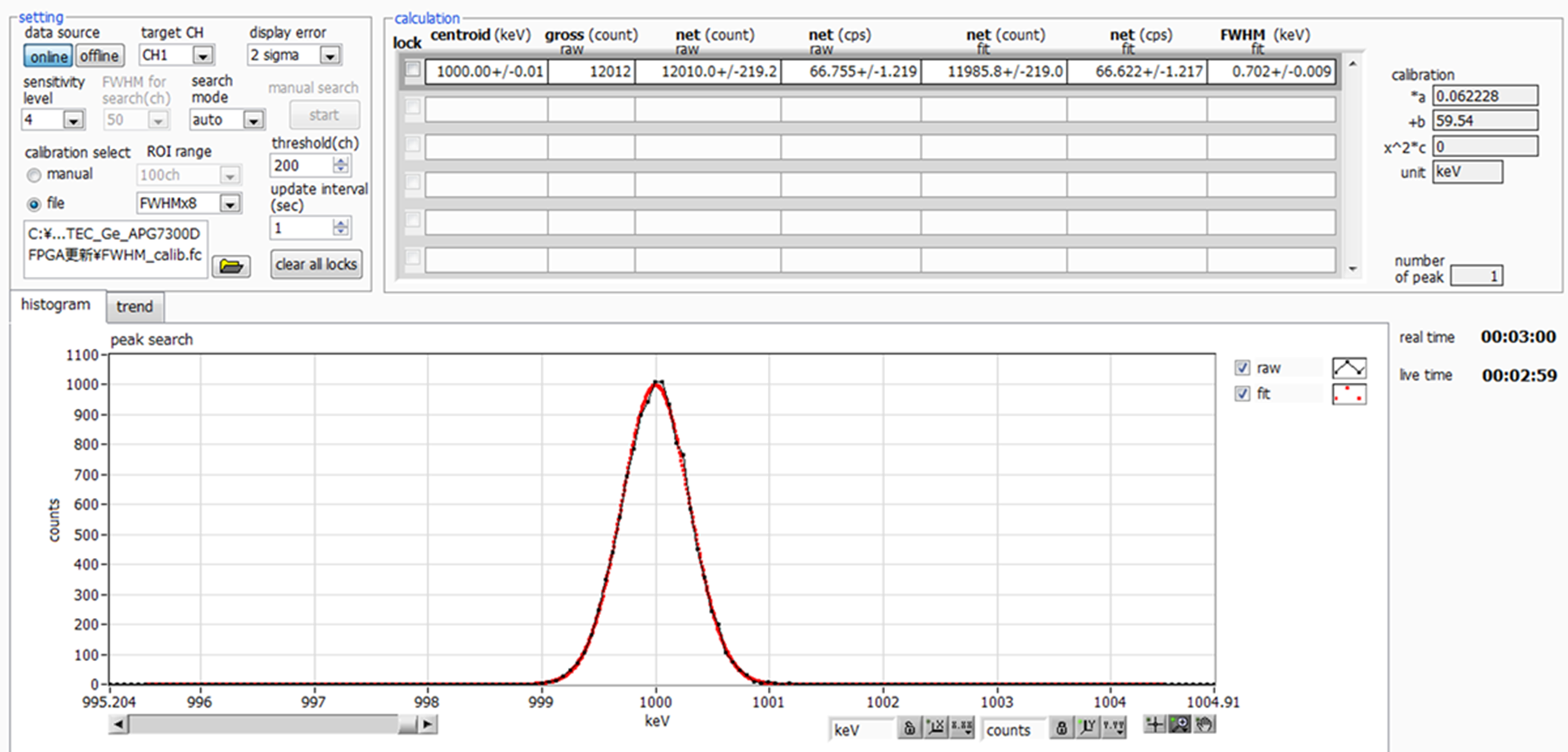
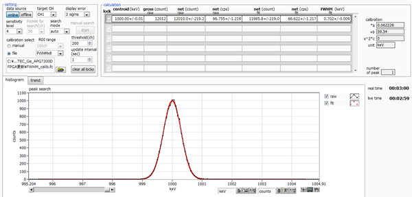
Shaping ampの時定数は2μs
APG1603 パルサーの分解能0.7keV
|
|
|
|
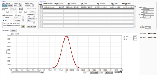
他社製品A パルサーの分解能0.945keV
|
|
|
|
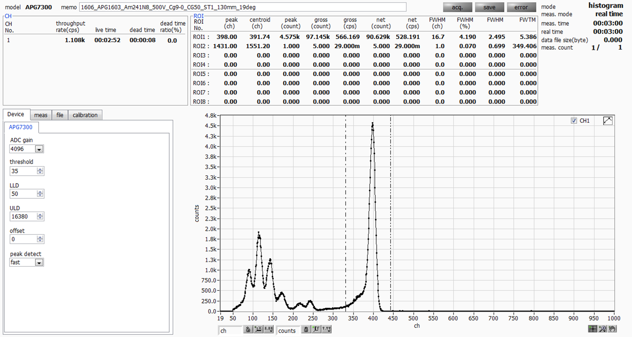
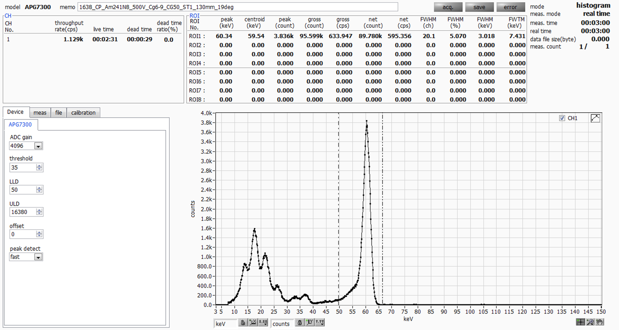
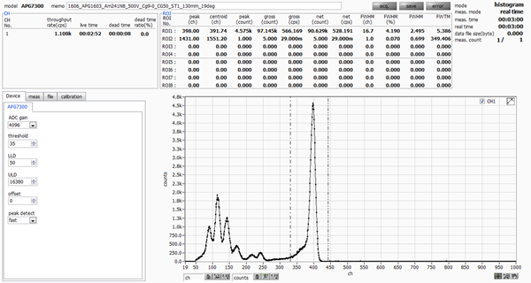
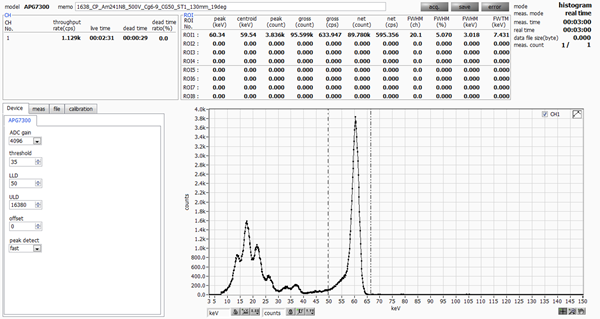
それでは、CdTe半導体検出器を使って実際にスペクトルを測定します。測定するピークはAm-241の59.5keVです。
|
|
|
|
Shaping ampの時定数は2μs
APG1603 59.5keVの分解能2.49keV (4.19%)
|
|
|
|
他社製品A 59.5keVの分解能3.01keV (5.07%)
|
|
|
|
測定結果は、 APG1603は分解能2.49keV (4.19%)、他社製品Aは分解能3.01keV (5.07%)となりました。カタログデータの0.75keVと1keVの差は実際の計測でも現れてきます。これは、半導体検出器ということや59.5keVと比較的低エネルギーだったことも思われますが、是非一度APG1603を使ってみてはいかがでしょうか。
それでは、より良い製品が作れるように社員一同全力で頑張ります。応援の程どうぞよろしくお願いします。
参考文献
[1] 岡村迪夫,インターフェイス, CQ出版社, 1976年2月号
[2] 松井邦彦, OPアンプ活用100の実践ノウハウ, CQ出版社, 1999年
[3] コワルスキー, 原子核エレクトロニクス, 朝倉書店, 1971年
|